
Inside the Blackwell SM: How NVIDIA Redesigned the Building Block of GPU Computing
I have been spending a lot of time in CUDA code lately, writing SGEMM kernels from scratch and benchmarking them on an H100. As I push closer to hardware limits, I keep bumping into the same question: what is the hardware actually doing underneath all this abstraction?
So I went back to the architecture diagrams and read through NVIDIA's Blackwell technical disclosures to understand what changed in this newest GPU generation and more importantly, why those changes matter for anyone writing GPU kernels.
Here is a plain-English walkthrough of what lives inside one Streaming Multiprocessor (SM) on a Blackwell GPU and how data flows through it during a matrix multiply.
The Big Picture: What Is an SM?
A GPU is not one giant processor. It is a collection of dozens (or hundreds) of small, independent compute units called Streaming Multiprocessors. An H100 has 132 of them. A Blackwell B100 has 170 of them.
Every SM is an entire mini-processor on its own with instruction schedulers, fast on-chip memory, general-purpose CUDA cores, and specialized matrix accelerators. All SMs run completely in parallel, each executing its own chunk of your computation at the same time.
A kitchen analogy helps make this concrete:
- Global Memory (HBM3e) is the giant wholesale warehouse across town: holds everything you need, but slow and expensive to travel to.
- TMA (Tensor Memory Accelerator) is the dedicated courier delivery van: moves entire crates of ingredients back and forth in the background while the chefs keep working.
- Shared Memory (SMEM, 228 KB) is the prep counter right beside the chefs: small, but instantaneous to grab from.
- Tensor Core (tcgen05) is a specialized industrial pasta maker: does one specific job (matrix multiply) at absurd speed.
- TMEM (Tensor Memory) is a dedicated holding rack right beneath the pasta maker: keeps all finished pasta organized without cluttering the chef's personal cutting board.
- Register File is the chef's personal tool belt: fastest access possible, but holds very few items.
- CUDA Cores are the versatile line cooks: handling peeling, seasoning, and sauce finishing (epilogues, activations, scaling, and biases).
What Lives Inside One SM
Here is the complete architectural layout of a single Blackwell SM:
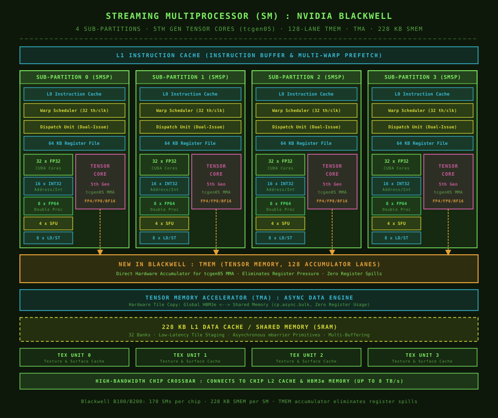
Every Blackwell SM is divided into 4 distinct sub-partitions (SMSP 0 through 3), each containing:
- L0 Instruction Cache and Warp Scheduler: tracks up to 32 threads per clock cycle and issues instructions with zero-overhead warp switching.
- Dispatch Unit: dual-issue dispatch logic feeding independent functional units.
- 64 KB Register File: 16,384 32-bit registers per partition, totaling 256 KB per SM.
- 32 FP32 CUDA Cores: single-precision floating point math.
- 16 INT32 Cores: integer arithmetic, pointer offsets, and index math.
- 8 FP64 Cores: double-precision scientific compute.
- 4 Special Function Units (SFU): transcendental math such as sine, cosine, square roots, and reciprocals.
- 8 Load/Store (LD/ST) Units: local and shared memory accesses.
- 5th Generation Tensor Core (
tcgen05): tile-level matrix multiply-accumulate supporting FP4, FP8, FP16, and BF16 formats.
Beneath the 4 partitions sit the SM-wide shared resources:
- TMEM (Tensor Memory): 128 dedicated accumulator lanes directly wired to the Tensor Cores.
- TMA Engine (Tensor Memory Accelerator): hardware asynchronous multi-dimensional tile copy unit.
- 228 KB L1 Data Cache and Shared Memory (SMEM): 32 memory banks with asynchronous barrier primitives.
- Texture Processing Units: surface reads and texture caching.
- High-Bandwidth Chip Crossbar: links the SM directly to the chip-wide 50+ MB L2 cache and multi-terabyte-per-second HBM3e stack.
Global Memory: The Warehouse
Global memory (GMEM) is the GPU's main RAM, implemented as HBM3e stacked directly alongside the Blackwell silicon interposer. On a Blackwell B200, this delivers up to 192 GB of capacity and 8 TB/s of bandwidth.
Even with 8 TB/s of bandwidth, accessing DRAM takes 400 to 600 clock cycles of latency. If your threads wait on DRAM for every arithmetic operation, the GPU spends over 90% of its time idling.
The goal of every optimization we build (block tiling, register reuse, vectorized loads) is to make visits to this warehouse as infrequent and as large-scale as possible.
TMA: The Dedicated Delivery Courier
In older architectures (Ampere and earlier), loading data from global memory into shared memory required individual thread instructions:
- Each thread computed its global memory address.
- Each thread issued a load instruction into a private register.
- Each thread wrote the register value into shared memory.
- Threads synchronized with
__syncthreads().
Hopper introduced and Blackwell expands the Tensor Memory Accelerator (TMA). Instead of hundreds of threads managing pointers and registers, a single thread issues one bulk descriptor instruction:
"Copy this 128x64 2D matrix tile from global memory address A directly into shared memory address B."
The TMA hardware executes the entire transfer autonomously, translating multidimensional tile coordinates, respecting bounds, and writing straight into shared memory without touching thread registers.
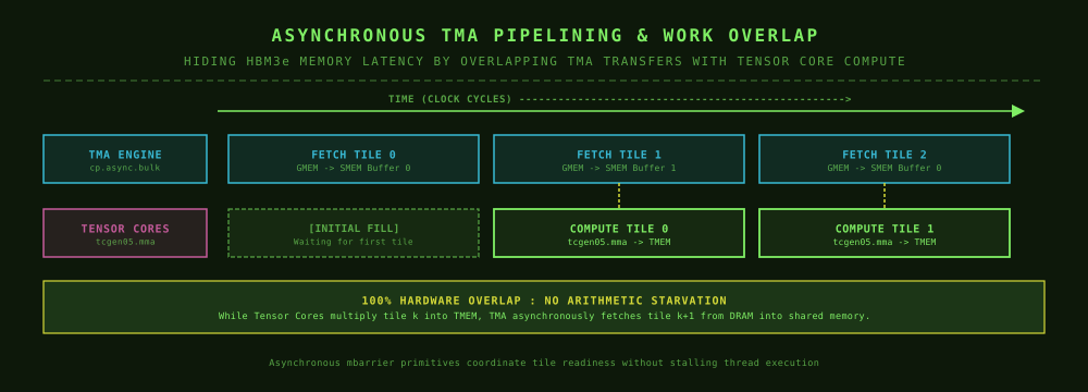
While TMA transfers tile k+1, the Tensor Cores compute on tile k. Software pipelining completely hides the hundreds of cycles of DRAM latency.
Shared Memory: The Counter Next to the Chefs
Shared memory is on-chip SRAM located physically inside the SM. On Blackwell, each SM provides 228 KB of configurable shared memory and L1 cache.
Shared memory delivers roughly 20 to 30 clock cycles of latency, an order of magnitude faster than DRAM. When threads tile their matrix inputs into shared memory, every element loaded from GMEM is reused tens or hundreds of times by the Tensor Cores, saving massive amounts of DRAM traffic.
TMEM: The Biggest Architectural Breakthrough
On every GPU generation before Blackwell (Volta, Turing, Ampere, and Hopper), the Tensor Core accumulator lived inside the register file.
Here is why that was a major problem:
When running a GEMM, the Tensor Core computes D = A x B + D. The output matrix D must be accumulated across all iterations of the K dimension. For an 8x8 tile fragment per thread, storing those partial sums requires up to 64 to 128 registers per thread.
When thread blocks consume 128 registers per thread, the SM runs out of register space immediately. The GPU scheduler cannot schedule enough concurrent warps to hide memory latency. Worse, when the matrix multiply finishes and the epilogue begins (bias addition, GELU or SwiGLU activation, scaling), the compiler frequently runs out of registers and spills intermediate values to slow local memory.
Blackwell introduces Tensor Memory (TMEM) to eliminate this bottleneck:
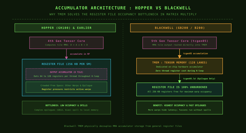
TMEM is a dedicated on-chip memory array composed of 128 accumulator lanes, physically coupled to the Tensor Cores:
- As
tcgen05.mmainstructions execute over the K dimension, partial sums accumulate directly inside TMEM. - The thread register file remains completely untouched during the entire main loop.
- All 256 KB of registers remain available for other warps, maximizing SM occupancy and latency tolerance.
- When the K loop completes, a
tcgen05.ldinstruction transfers the final result into registers for epilogue processing.
The GEMM Data Path from Start to Finish
Now we can trace the entire lifecycle of a matrix multiply through a Blackwell SM:
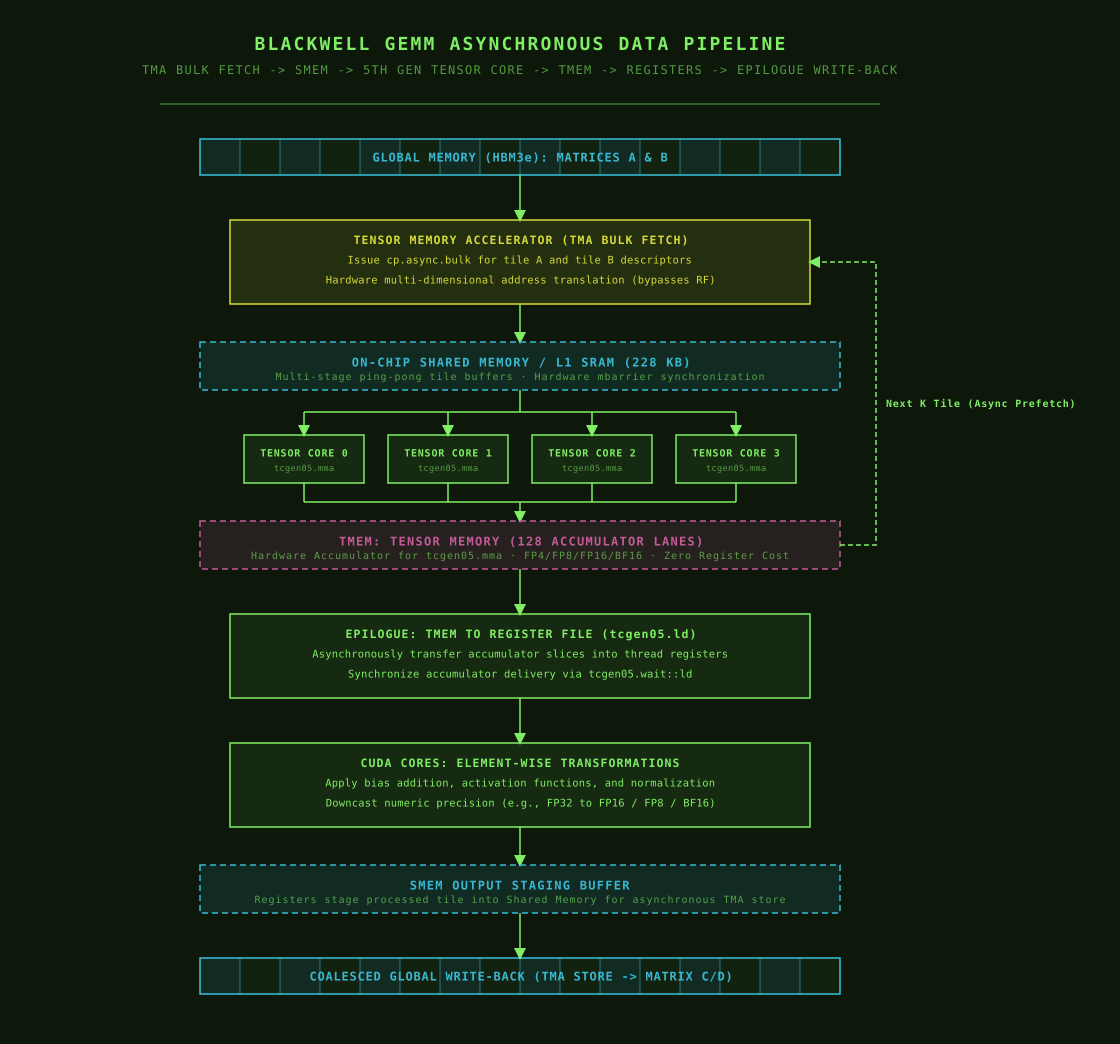
Follow the execution step by step:
- Global to Shared Memory: The TMA engine issues asynchronous bulk copies (
cp.async.bulk) to load tiles of matrices A and B from HBM3e directly into 228 KB SMEM ping-pong buffers. - Shared Memory to Tensor Core: The 5th generation Tensor Cores read operand tiles from shared memory through high-bandwidth internal crossbars.
- Tensor Core to TMEM: The Tensor Core executes
tcgen05.mmainstructions, accumulating partial products directly into the 128 lanes of TMEM across the full K dimension. - Pipelined K Iteration: While the Tensor Core is multiplying tile
k, the TMA is already prefetching tilek+1into the alternative SMEM buffer stage. - TMEM to Registers (
tcgen05.ld): Once the K loop finishes,tcgen05.ldtransfers the accumulated result tile from TMEM into the thread Register File, synchronized withtcgen05.wait::ld. - CUDA Core Epilogue Transformations: CUDA cores execute element-wise operations on the register data: bias addition, RMSNorm, activation functions (GELU, ReLU, SwiGLU), and FP32 to FP8 or BF16 quantization.
- SMEM Output Staging: Threads write the processed register fragments into an SMEM output staging buffer to enable coalesced hardware memory copies.
- Asynchronous Write-Back to Global Memory: The TMA engine issues an asynchronous bulk store (
cp.async.bulk.tensor) to transfer the finalized matrix C tile from SMEM back into HBM3e memory.
Why This Architecture Changes CUDA Kernel Design
Understanding the Blackwell SM clarifies why modern GPU kernel engineering is moving away from manual thread-level math loops toward asynchronous hardware pipelines:
- Block tiling stages DRAM data into 228 KB SMEM to avoid GMEM latency.
- TMA bulk transfers replace thousands of thread load instructions with autonomous hardware memory engines.
- TMEM decouples compute from register allocation, allowing kernels to use deep multi-stage software pipelining without suffering from register pressure or low occupancy.
- tcgen05 Tensor Cores deliver peak arithmetic density for FP4, FP8, FP16, and BF16 formats, while CUDA cores focus purely on non-linear epilogues.
Every piece of the Blackwell SM exists to solve a specific data movement or storage bottleneck, ensuring the arithmetic units never starve for data.
Quick Reference: SM Hardware Units
| Unit | Location | Primary Role | Key Hardware Detail |
|---|---|---|---|
| GMEM (HBM3e) | Off-chip stacked DRAM | Massive matrix storage | Up to 192 GB, 8 TB/s bandwidth, 400+ cycles latency |
| TMA Engine | On-chip per SM | Asynchronous bulk memory copies | Hardware multi-dimensional tile copy, bypasses registers |
| Shared Memory (SMEM) | On-chip per SM | High-speed tile staging | 228 KB SRAM, 32 banks, mbarrier synchronization |
| Tensor Cores | 4 per SM (1 per partition) | Matrix Multiply-Accumulate (MMA) | 5th Gen (tcgen05), supports FP4, FP8, FP16, BF16 |
| TMEM | On-chip per SM | Dedicated Tensor Core accumulator | 128 lanes, stores output D tiles, frees register file |
| Register File | 64 KB per sub-partition | Thread-private working storage | 256 KB total per SM, zero-cycle access |
| CUDA Cores | 128 FP32 per SM | General-purpose arithmetic | Handles epilogues, scaling, bias terms, activations |
About the author
Ritesh Yadav works as an AI/ML Engineer. He writes independent research notes on ML performance, infrastructure, and systems, covering CUDA, low-latency inference, generative AI, distributed training, Kubernetes, and LLMOps.